Journal of Fluid Flow, Heat and Mass Transfer (JFFHMT)
ISSN: 2368-6111

Volume 8 - Year 2021 - Pages 135-146
DOI: 10.11159/jffhmt.2021.015
Characterization and Modeling of Surface Roughness on a Silicon/PZT Unimorph Cantilever using Finite Element Method
Jean Marriz M. Manzano1, Magdaleno R. Vasquez Jr2, Marc D. Rosales1, Maria Theresa G. de Leon1
1University of the Philippines, Electrical and Electronics Engineering Institute
Quezon City, Philippines, 1101
jean.manzano@eee.upd.edu.ph; marc.rosales@eee.upd.edu.ph; theresa.de.leon@eee.upd.edu.ph
2University of the Philippines, Department of Mining, Metallurgical and Materials Engineering
Quezon City, Philippines, 1101
mrvasquez@up.edu.ph
Abstract - Silicon etching using deep reactive ion etching (DRIE) at large etch depth results in rougher surfaces due to increased response in process pressure, amount of coil power, increased amount of helium leak at the backside, and even post process handling. To account for the effects of surface roughness on the characteristics of a silicon cantilever beam, a numerical model based on the finite element method (FEM) modeling was developed using actual roughness data from fabricated samples. The acquired roughness data was integrated to the silicon cantilever beam model coupled with multiphysics to simulate a piezoelectric energy harvester. Simulation result shows that roughness parameter ranging from 1.488-3.138 μm can shift the resonant frequency by 5.53% to 9.48% or 308.31 Hz to 551.21 Hz of the device but does not have significant effect on the output power. The significant shift in the resonant frequency implies that careful consideration of surface roughness from fabrication processes must be considered when designing energy harvesters.
Keywords: Microelectromechanical systems, deep reactive ion etching, surface roughness, finite element method, multiphysics analysis, vibrational energy harvester.
© Copyright 2021 Authors - This is an Open Access article published under the Creative Commons Attribution License terms Creative Commons Attribution License terms. Unrestricted use, distribution, and reproduction in any medium are permitted, provided the original work is properly cited.
Date Received: 2020-12-25
Date Accepted: 2021-01-11
Date Published: 2021-03-02
1. Introduction
Critical fabrication processes like the deep etching of silicon in microelectromechanical systems (MEMS) devices cause surface irregularities. These nonidealities are caused by the plasma etch process with variables like radio frequency power, chamber pressure, etch gas flow rates, and temperature, affecting etch rate. Other factors that contribute to these nonidealities are laboratory-type clean rooms where the environment is not as controlled as in a manufacturing facility, less maintained polishing tools and equipment, non-DRIE etching tool of lower aspect ratio, and post-etch device handling; hence, making it even more difficult to keep the surface uniform. A specific example in MEMS fabrication, is when flow rates of SF6 and C4F8 gases influence the trench morphology. The gas flow rates can affect surface roughness depending on the etching rate, sidewall angle, and sidewall damage [1]. The roughness warp formed from this process may cause significant effects on the geometry of the device and may shift the resonant frequency. These surface irregularities influence not only the surface properties of a device but also its reliability and performance [2]. For cantilevers that are used for energy harvesting, this may lead to harvesting inefficiency as its operating frequency is highly dependent on its geometric shape.
Prior to fabrication, it is essential to have a good model of the device to aid its design and development. Moreover, effects of surface roughness to a device must be incorporated in the early design stages to improve its reliability, performance, and optimize its design.
Many works on modeling surface roughness are made for MEMS sensors [3], switches [4], and optical devices [5] but not for energy harvesters. With the growing use of ubiquitous internet-of-things (IOT) and wireless sensor network (WSN) devices in the next few years [6], the demand for battery to power these devices will increase as well. These devices must be autonomously powered using unlimited source of energy through MEMS energy harvesters. MEMS energy harvesters allow miniaturization of mechanical structures to be integrated with electrical circuitry however, its operating frequency is very much dependent on their form factor. Most of the existing models for roughness topography was created manually, analytically, script coded, independently studied, and are empirical [4,7-10]. Some have roughness models that were developed from experimenting several times through fabrication, which is tedious and costly [11]. Recent developments lack multiphysics analysis with roughness integrated to the device models [13-17]. Multiphysics analysis solves for coupled multiphysics phenomena simultaneously that may involve electrical, physical, mechanical, structural, chemical and optical stimuli.
Previous studies on the effects of surface roughness on RF MEMS capacitive switches showed a reduction of the down-state capacitance that shifts the resonant frequency of the switch [9]. Leakage current and actuation voltage shift due to dielectric charging are increased by orders of magnitude compared to a planar contact [8]. Meanwhile, introduction of roughness to optical nanoantenna and carbon nanotubes results in a shift in the resonance wavelength [18], and an underestimated material property compared to a smooth model [11], respectively. To our best knowledge, the FEM model with realistic surface roughness on energy harvesters has not yet been investigated in literature.
The succeeding section of this paper is organized as follows. Section 2 discusses fabrication processes of samples used to acquire surface roughness. Followed by section 3 that discusses on how the roughness were characterized and analyzed. Section 4 shows a brief explanation of the numerical model used to compare with the FEM simulated model. Section 5 presents the process of how the FEM cantilever model was built. Section 6 discusses the simulation of the FEM model. Lastly, Section 7 concludes the research work.
2. Fabrication of silicon samples
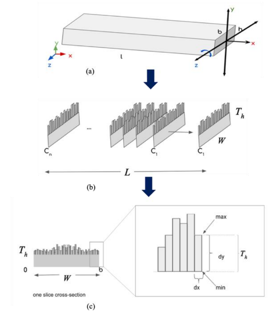
Before developing the FEM 3D model of the cantilever beam’s surface roughness, actual samples were microfabricated for roughness characterization. The fabrication process investigated in this paper is deep reactive ion etching (DRIE) of silicon. The full fabrication was basically subdivided into four major processes [12]: wafer cleaning, oxidation, photolithography, and etching, as illustrated in figure 1.
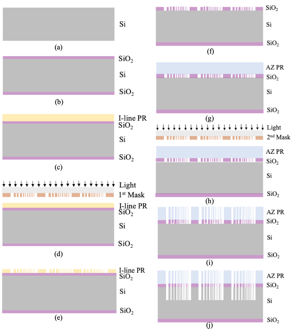
A 6” P-type test silicon wafers was RCA-cleaned represented in figure 1a and wet-oxidized to deposit an oxide of 280-300 nm thickness in figure 1b. The mask pattern that was used in this fabrication has trenches with widths of 2 µm up to 1000 µm and was replicated at the center, left, right, top, and bottom regions of the wafer to characterize process variations. The different steps of the two-photolithography processes are shown in figures 1c-1e and figures 1g-1i. For the process in figures 1c-1e, the substrate with 280-300 nm of silicon dioxide from wet thermal oxidation was coated with 1.2 µm of I-line photoresist (OiR906 1.2 µm). Then, the wafer was exposed using a 50 µm gap of soft-contact exposure under UV I-line intensity of 12mW/cm2 for 15s. After the post-exposure hard bake, the I-line photoresist was developed by spraying MF26A developer for 5s at 300 rpm and was hard-baked to harden the patterned photoresist for 70s at 230°C. After oxidation and pertinent photolithography steps, the oxide was etched at a rate of 0.3 µm/min. The etched part of the wafer was measured using nano spectrometer to ensure all exposed oxide were etched.
The depth of the silicon structure that must be etched is 550 µm. In order to have a better pattern transfer fidelity and avoid mechanical stress and cracks, a second coating of the wafer was done using the thick resist (AZ P4620 12 µm) as illustrated in the photolithography process in figures g-1i. To remove some bubbles that were observed on the photoresist after exposure, post-exposure hardbake was done at 120°C for 30s, followed by rehydration for 30 minutes. Then, these wafers underwent DRIE using a standard recipe with 1:10 ratio of O2 to SF6 and was bonded to a handle wafer to prevent an etch-through that might damage and contaminate the chuck of the chamber. A dummy wafer was placed under the sample wafer poured with 2.5 mL of Santovac®. The two wafers are bonded and was baked for 10 minutes on a hotplate. This newly bonded wafers were then placed in the DRIE etch system plasma chamber. The standard recipe to etch 300 µm deep is equivalent to at least 100 cycles. Etching characterization was performed to get the needed depth of 520-550 µm in which etch cycle is equivalent to 600 cycles. Etch depth was measured using OLS5000 3D laser microscope.
3. Characterization of Surface Roughness
The DRIE technology gives high-aspect ratio (HAR) etch and minimal roughness [11]. In order to acquire the roughness data caused by deep-etching, the samples were measured using a high-resolution 3D-laser microscope. To properly characterize surface roughness, roughness parameters were identified through the analysis of the measured surface roughness. The measured roughness data was used for FEM modeling of the cantilever beam with surface roughness.
3.1 Measurement Apparatus
Surface roughness evaluation was performed by using laser microscopy. This method has several advantages: (1) it can measure finer roughness, (2) non-abrasive, (3) fast and precise, (4) high resolution, and (5) offers wide-field measurement over conventional stylus measurements, scanning probe microscopes, and scanning interferometers. This method is adapted to determine the roughness of the DRIE-processed surface.
To capture surface roughness, an appropriate objective lens was selected. The data acquisition application software of OLS5000 was used to capture
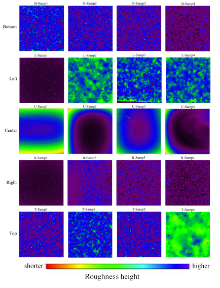
the live image of the sample. The image was acquired by imaging the reflected light of the laser beam that is irradiated on the sample. Then, the sample’s region of interest was captured using numerical aperture of 0.45 of the objective lenses with 20x magnification. The maximum pixel size used to fit the region of interest for imaging was 640 x 640 µm2. Image correction was also performed to remove the tilt that could possibly give inaccurate roughness data. The acquired height image per region is shown in figure 2.
3.2 Roughness Parameters
Examination of the measured topographical data of the sample’s surface were made using OLS5000 data analysis application. Characterization of the samples’ surface roughness was done by estimating the root mean square, Sq, and the centreline average, Sa , of the evaluation area. Additionally, parameter Ssk was used to measure the profile’s skewness and parameter Sku for quantifying kurtosis. These four amplitude parameters were used to describe the samples’ surface.
Sq was chosen to be one of the roughness parameters as it has more statistical significance than Sa and has more stable results since it is not influenced by scratches. Sq represents the standard deviation of surface height and is more sensitive than Sa [13]. Aside from that, Sq is a widely used parameter because of its ease of use. Another advantage of the parameter Sq overSa is that when height variations become higher, Sq gives better and dependable statistical values of the distribution where parameter Sa becomes less reliable.
Another amplitude parameter that was used is the parameter Ssk. This parameter is used to measure profile symmetry. If the skewness is leaning towards a positive value, it indicates a deviation to the lower side. If it is leaning towards a negative value, it indicates deviation to a higher side. Meanwhile a skewness of zero value signifies a uniform height distribution. Moreover, skewness is used to differentiate surfaces having the same Sa values but with different shape.
The last parameter used is Sku. This parameter indicates presence of disproportionate high peaks or deep valleys of a surface texture if Sku > 3.00. A normally distributed height of a surface Sku =3.00, while for varying surfaces with no extreme peaks or valley features, it has Sku < 3.00. This parameter also tells the heaviness of the distributions’ tail and is useful for indicating presence of unusual peaks or valleys that may occur on a surface.
3.3 Roughness Analysis
The image of the DRIE sample was captured under a high-resolution microscope in an ambient environment. The scan size was initially determined by doing measurement runs. This was done by selecting a bigger scan size at first and the measured roughness, Sq, was compared in between regions. It was estimated that if the measured roughness is greater than 5 µm, the scan size was decreased further since in DRIE process, roughness usually ranges from nanometer to a few microns only. Then, the captured image of the region of interest was processed by removing noise and tilt to make sure that roughness is measured instead of waviness or lay.
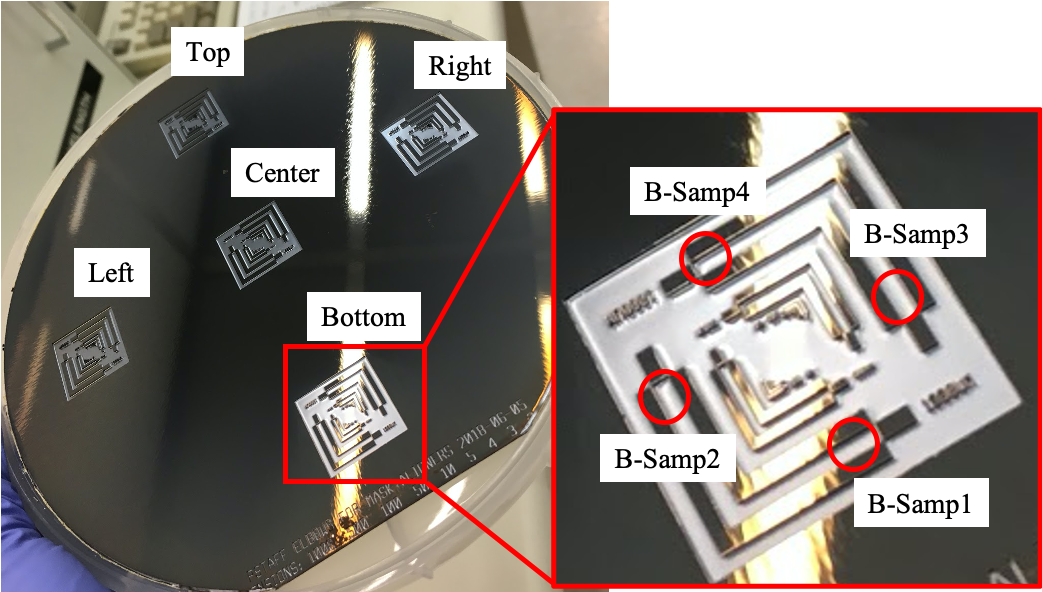
Before roughness was analyzed, the etch depth was measured to ensure that the roughness information was from the target depth of 550 µm. The same measurement process was performed on all four samples per wafer region as shown in figure 3. Depth measurement was found to have a range of 540-590 µm.
The statistical information was also acquired. For a fair quantification of surface roughness, the data that was selected was ensured to be at the same thickness, i.e., the depth of the etch is almost equal.
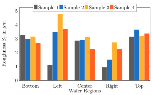
The captured roughness was quantified using parameters Sq, Ssk, and Sku. Across the wafer, Sq ranges from 1 μm to 4.7 μm as shown in figure 4. It can also be observed that the center region of the wafer tends to have an average Sq of approximately 2.8 μm.
Meanwhile, the left and right regions have more variations compared to the bottom, top, and center regions. This variation can be caused by post-process handling of the etched material, ion, and neutral transport in the plasma [14], micro loading [15], and process parameters reported in [16] that affects the etching properties of the plasma etcher.
The parameters Ssk and Sku are used to quantify the roughness distribution in a measured area. In figure 5, the Ssk data gathered from a DRIE-etched wafer shows a roughness height distribution that is skewed below the mean for all regions at some degree. The left and right regions have an average skewness of 1.589 and 2.271, respectively, and have higher skewness than the bottom, center, and top regions wherein the skewness average is approximately 1. The positive sign of Ssk indicates the prevalence of peaks. As seen in figure 5, the skewness of sample 1 in the left region shows the highest value among all samples.
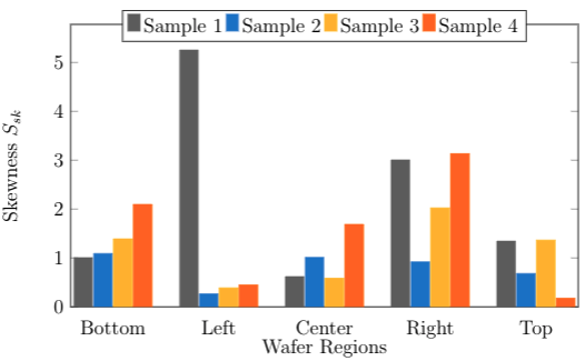
The value measured by skewness and kurtosis is dependent on the effects of the surface properties and how the surface was imaged and measured. Like any other imaging technique, it is suspected that the possibility of image artifacts causes this increase in skewness. These artifacts are induced by several factors, such as processing the digital data, a limited number of excitation wavelengths for laser microscopes, poor operating environment, and fabrication processes to the sample. Other areas of the left and top regions show a more normally distributed roughness height compared to other regions, as illustrated in figure 5. It is also observed that sample 1 of the left and right regions has a narrow distribution than the other three. Moreover, the bottom and top regions have almost the same distribution range compared to the left, center, and right regions. This distribution deviation is mainly due to the micro-machining process. DRIE uses plasma ions to bombard and react with the surface causing the materials composing the surface to be etched. The gas chemistry dictates the etching effectivity of the process, and other parameters such as coil power, process pressure, and helium backside cooling are responsible for the generation of surface roughness [17].
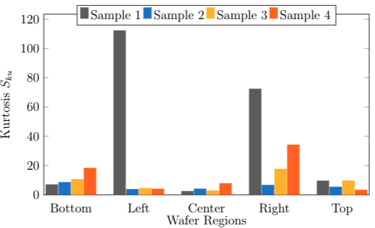
The parameter Sku is used to measure the heaviness of the tail of distribution or signifies outliers. Figure 6 shows both sample 1 of the left and right regions has the highest kurtosis value, and by visual inspection, these two samples’ distribution has a narrow shape. Meanwhile, other regions’ distribution shape is shown to be wider as compared to the left and right regions. The same reason causes this difference with skewness as the distribution’s data represents the captured roughness image’s statistical information.
4. Numerical Modeling of Surface Roughness
The roughness information in the previous section was used in the numerical model implemented in MATLAB [12]. Using the analysis of surface roughness as varying heights, the cantilever beam in figure 7a was subdivided equally as one slice of the cross section, Cn, in figure 7b. The cross-section was decomposed into uniform dx segments that runs along the width of the beam where Hmax and Hmin defines the maximum and minimum height of each captured image in figure 2. Then, the area moment of inertia in equation 1 was calculated.

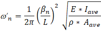
The resulting area moment of inertia was used in equation 2 to compute for the natural frequency of a cantilever beam with surface roughness.
This developed numerical model was compared to the FEM model that will be discussed in the next section.
5. FEM Modeling of Surface Roughness
The roughness data from the measurements were incorporated in the 3D device model in the COMSOL Multiphysics tool through parametric surface and interpolation functions. A basic cantilever beam in d31 mode geometry was built using COMSOL. The geometry primitives of the model’s spatial dimension are based on the state-of-the-art designs for piezoelectric energy harvesters. The equivalent area of the captured roughness from the fabricated sample was multiplied by 5 x 2 (length and width) to fit the size of the beam, which has dimensions equivalent to 5120 μm x 1280 μm or 8192 pixels x 2048 pixels. This is to represent roughness being present all throughout the beam’s surface. Meanwhile, the height was set to 101.9 μm - the total height of the combined layers of the beam, oxide, PZT and electrodes.
For this study, only the silicon beam was considered to have roughness and the rest of the layers was set to be smooth. MEMS, structural mechanics, multiphysics, and AC/DC modules were used for the electrostatic interface, structural analysis and electrical simulations.
5.1. 3D Multiphysics Device Modeling
The processed roughness image in MATLAB was integrated to the 3D beam FEM model in COMSOL. The cantilever beam with uniform thickness was created with the use of multiphysics to interface the structural mechanics governing the beam, as well as the other physics needed to simulate a piezoelectric energy harvester with integrated roughness. The 3D cantilever beam general flow modeling process in COMSOL is shown in figure 8.
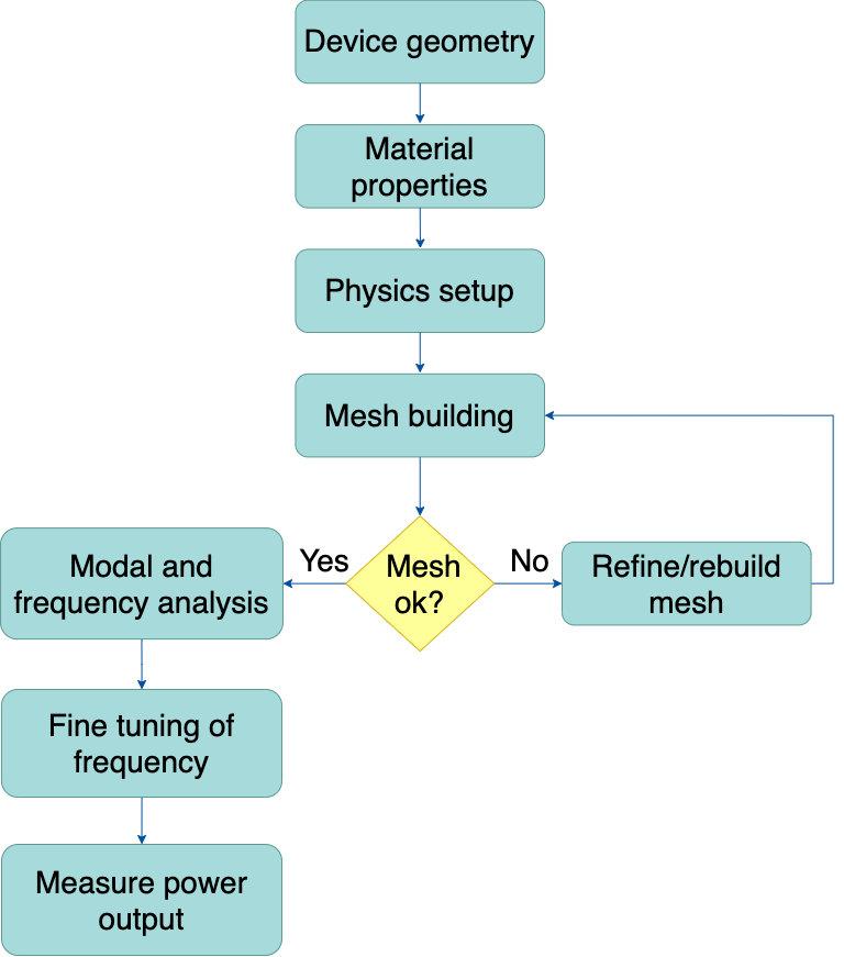
5.2. Device Geometry
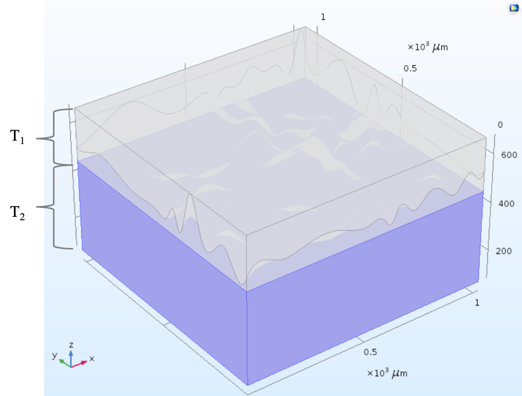
The structure that was built is the basic silicon cantilever beam. The beam’s dimension was set to a length and width of 5120 x 1280 µm 2. The thickness was set to 120 µm as the total height of the cantilever beam. The 20 µm serves as an allowance to the roughness geometry that will be subtracted from the combined block in figure 9. Initially, the upper T1, representing surface roughness, was set to zero and the lower T2 layer, representing the beam thickness, was set to 100 µm to simulate and verify a simple model of the ideal beam that will be used to compare with a beam with non-uniform thickness. After knowing the ideal beam frequency, the roughness data was incorporated to the multiphysics 3D model.
The CSV file of the roughness image was formatted into a table format text file in python so that it can be imported and read by the COMSOL Multiphysics software. The complete process of the importation and thickness set-up of the height data is shown in figure 10.
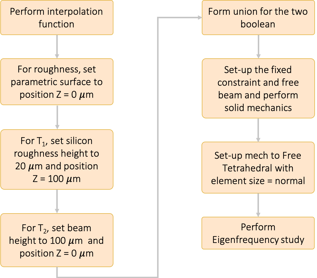
An interpolation function was used to describe and display the varying heights of the imported text file. It was observed that the rendered image in COMSOL was not the same as the 2D image acquired from the 3D high-resolution microscope but looks similar. This difference is caused by how the image data was interpolated and rendered in COMSOL. To verify that the same image information was used, the mean of the image was calculated in Matlab and was compared with the mean from the data analysis software of OLS5000. Therefore, regardless of the difference of the rendered image, the information was ensured to be the same. All images used in this study went through the same process and was saved as an individual interpolated function file integrated to the beam.
As the underlying data of roughness is now available in the model through the interpolation function, the actual shape of the beam with roughness was created. The parametric surface of the roughness was bounded inside a box to encapsulate the full height of the beam. This was done to be able to perform a geometry operation such that the parametric surface can be united with the bounding box. This node is responsible for the generation of the 3D image defined at a specific surface area. The expression for the parametric surface was described by the minimum and maximum x and y values of the surface area including the interpolated data for the z values in microns. The position of the parametric surface was placed at z = 0 μm, which is the boundary of T1 and T2 . The purpose of this is to bound the parametric surface within a rectangular block so that the upper entity of the geometry can be removed, resulting in only the roughness with Sq value ranging from 0.9 to 4.7 μm to remain on the surface of the beam. The silicon’s T1 and T2 layers ’ position are also defined before doing the boolean operation to form the union of the two separate blocks.
After integrating the surface roughness T1 to layer T2, other layers were added as well to be able to measure a potential difference across the material. The piezoelectric effect causes the generation of electric charge during deformation of the beam. This basic cantilever beam in d31 mode was created using different materials from COMSOL’s material library. Different layers and their thicknesses were added to the silicon beam. Moreover, this 3D model assumes the other layers are uniform and ideal as these layers are very thin. The change in resonant frequency caused by the added layers is also considered insignificant to the cantilever beam’s frequency shift due to roughness. This is because the analysis of the effects of surface roughness must come from the added roughness to the beam’s surface and not with the added layers.
5.3. Material Properties
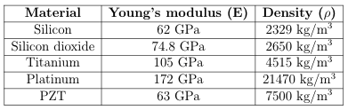
To completely define the piezoelectric energy harvester beam, different materials were added and assigned to the corresponding geometric entities or domains of the model. Since the fabricated samples are silicon, the setup used silicon for the beam, both for its smooth and rough portions. The material properties of each layer of the modelled cantilever beam are tabulated in Table 1.
Table 1: Material properties per layer of the FEM 3D model.
5.4. Physics Setup
The mechanical and electrical modules were used to build the physics setup that describes the physical phenomena governing 3D model of the energy harvester. Boundary conditions of the beam’s free end was set by selecting the concerned domains to ensure that no constraints and loads are acting on the boundary. The displacement field and structural velocity field was set to zero as an initial condition for transient simulation. Lastly, for the body load, a force per unit volume (N/m3) was selected to divide the total force of the 3D model’s selected domain equally throughout its entire body.
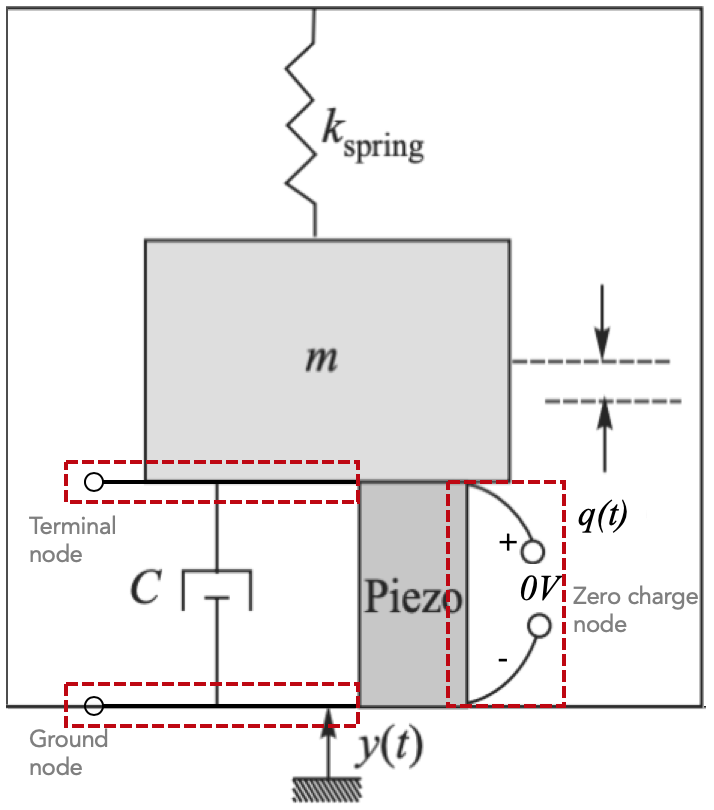
For the piezoelectric effect, piezoelectric multiphysics and the piezoelectric charge conservation was coupled in the electrostatics interface. A fixed constraint node was added to make the geometry entity fully constrained. This was done to set the boundary condition of the beam’s displacement to be zero in all directions. The charge conservation node was added to provide an interface in defining the constitutive relation and its associated properties according to Gauss’ law. A zero-charge node was used to set the condition of the charges on the boundary to be zero. This setting blocks any displacement field that can affect the boundary.
The initial values node was also added for setting the initial condition of the electric potential, V for transient simulation, which has a default value of zero.
The charge conservation, piezoelectric node was used as a coupling node to piezoelectric effect. This node is added by default to the electrostatics interface when a piezoelectricity interface is added. Without this node, the material behaves like a dielectric, not piezoelectric. Ground node was used to implement a zero potential of boundary condition V= 0. Lastly, a terminal node was added to provide a boundary condition for external circuits connection which is shown in figure 11.
A multiphysics module was used to simulate the piezoelectric effect on the modelled device, which requires coupling of both solid mechanics and electrostatics. After setting the physics, selection of domain was done to select applicable domains. The domains that have already been defined with other boundary conditions, material, or physics, that does not apply with the piezoelectric effect has been excluded. This is to ensure that the coupled physics is adapted only to the selected domains that is under study.
5.5 Mesh Building
Using the exact roughness data incorporated to the cantilever’s 3D device model in COMSOL, meshes were built for each beam to be able to run FEM simulations that solves for the beam’s eigenfrequency. FEM was used to compute for the approximation of the solution of the cantilever beam’s numerical model equations. The mesh of the model can be refined for two main reasons: (1) geometrical – for better representation of smaller elements and (2) mathematical - accuracy in solving by the use of denser meshes. The division of the model’s geometry was defined through mesh building. This includes the shape, element type, size, density and number of elements of the mesh that affects the computation time of the problem. An example of a meshed geometry is shown in figure 12.
The boundaries defined in the geometry are discretized into mesh elements. These mesh elements represent the nodal representation of the geometry and functional representation of every domain. These meshes are based on FEM where differential equations of each element are computed. The sample scaled geometry in figure 11 shows a complex shape and can be meshed with tetrahedrons. Therefore, tetrahedral elements with minimum element size of 92.2 μm and maximum element size of 512 μm are
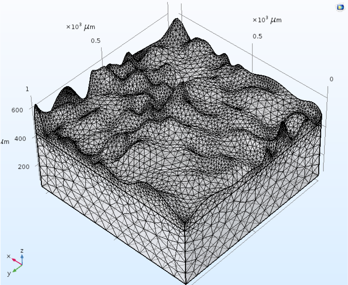
chosen to create the shape of the 3D geometry. The element size of the mesh was calibrated for general physics since the cantilever beam model does not deal with fluid flow or plasma. The rest of the body generated the mesh successfully except for some faces of the rough surface.
This was resolved by iteratively and systematically changing the number of knots and adjusting the tolerance when recreating the mesh. Increasing the maximum number of knots help enhance the representation of the surface. Increased number of knots also improve the chance to achieve a tighter relative tolerance. The maximum number of knots for the cantilever beam was increased to 400 which improves tighter relative tolerance. This was set for all beams. However, for other geometries (having different roughness) this tolerance value became difficult to reach. Therefore, a new relative tolerance was set for such beams.
Different mesh type was also explored to simulate an ideal beam having a size of 5120 x 1024 x 50 μm3. These are the coarser, coarse, normal and fine mesh sizes. All four mesh sizes were used to know the change in frequency that each different mesh type contributes. The simulation for each mesh size resulted in a frequency of 2666.2 Hz (coarser mesh), 2663.8 Hz (coarse mesh), 2662.6 Hz (normal mesh), and 2661.6 Hz (fine mesh). From this frequency values and this specific geometry, we can conclude that as the mesh type changes, the frequency also changes but insignificantly. It is expected however that the finer the mesh is, it is closer to the actual frequency that is calculated because there are more PDEs computed for each node that represents the geometry. This is also true for the beams with roughness as its geometry is too complex. In this case, the normal mesh was used for all beam’s simulation. As for some parts of the geometry of the beam with roughness that exhibits meshing error, meshes were refined to resolve the degeneration of the triangle. This step was repeated until meshing conditions are all satisfied.
6. Simulation of the cantilever beam
An eigenfrequency analysis was performed to scan the different mode shapes of the beam using eigenfrequency study. From this analysis, the first mode shape was used in fine tuning the device’s frequency by doing frequency sweeps. These frequency steps were manually tweaked to resolve peaks or resonances. Equation 2 in section 3.3 solves the natural frequency of a beam using a non-dimensional frequency β, which corresponds to an eigenmode of a normalized deformed shape at its eigenfrequency. In COMSOL, only the first eigenfrequency was computed and used. Figure 13 shows the simulated beams with almost the same thickness and its roughness data. Resulting frequency of the simulation is tabulated in Table 2.
Table 2. Equivalent frequency and power to each sample with roughness at 100 µm thickness.
| Sample | Roughness (Sq) | Simulation (Hz) |
| Ideal | 0 | 5340.7 |
| R-Samp2 | 1.488E-06 | 5646.8 |
| B-Samp4 | 2.683E-06 | 6728 |
| R-Samp3 | 2.724E-06 | 5745 |
| T-Samp1 | 3.138E-06 | 5879.9 |
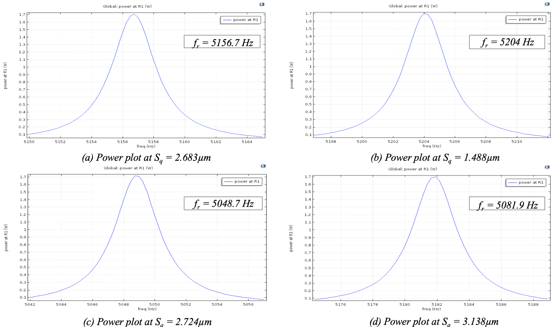
The output power of the same beam was also calculated from the voltage induced across the piezoelectric subjected to acceleration. An electrical load of 1000 Ω W was connected to the terminal and ground node, with an applied force of 0.001N. From the plot shown in figure 14, each peak power occurs at the resonant frequency of each beam with different roughness profile data. At a load of 1000 Ω, the maximum power is approximately 1.7 W.
The change in Sq values does not significantly affect the harvested power as power is not entirely dependent on the geometry but on the mechanical and electrical damping coefficients. Table 3 lists a summary of the output power results.
Table 3. Equivalent frequency and power to each sample with roughness at 100 µm thickness.
| Sample | Sq ( μm) | Eigenfrequency (Hz) | Resonant Frequency | Power (W) |
| Ideal | 0 | 5192.4 | 5196 | 1.7046 |
| R-Samp2 | 1.488E-06 | 5200.6 | 5204 | 1.7013 |
| B-Samp4 | 2.683E-06 | 5879 | 5156.7 | 1.7095 |
| R-Samp3 | 2.724E-06 | 5045.4 | 5048 | 1.7178 |
| T-Samp1 | 3.138E-06 | 5178.3 | 5181.9 | 1.7008 |
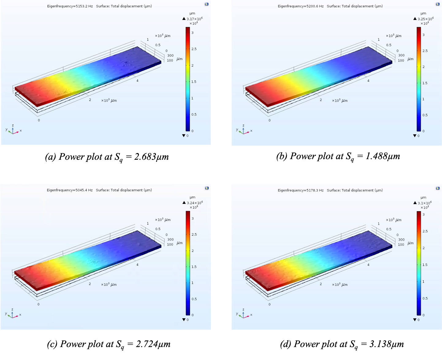
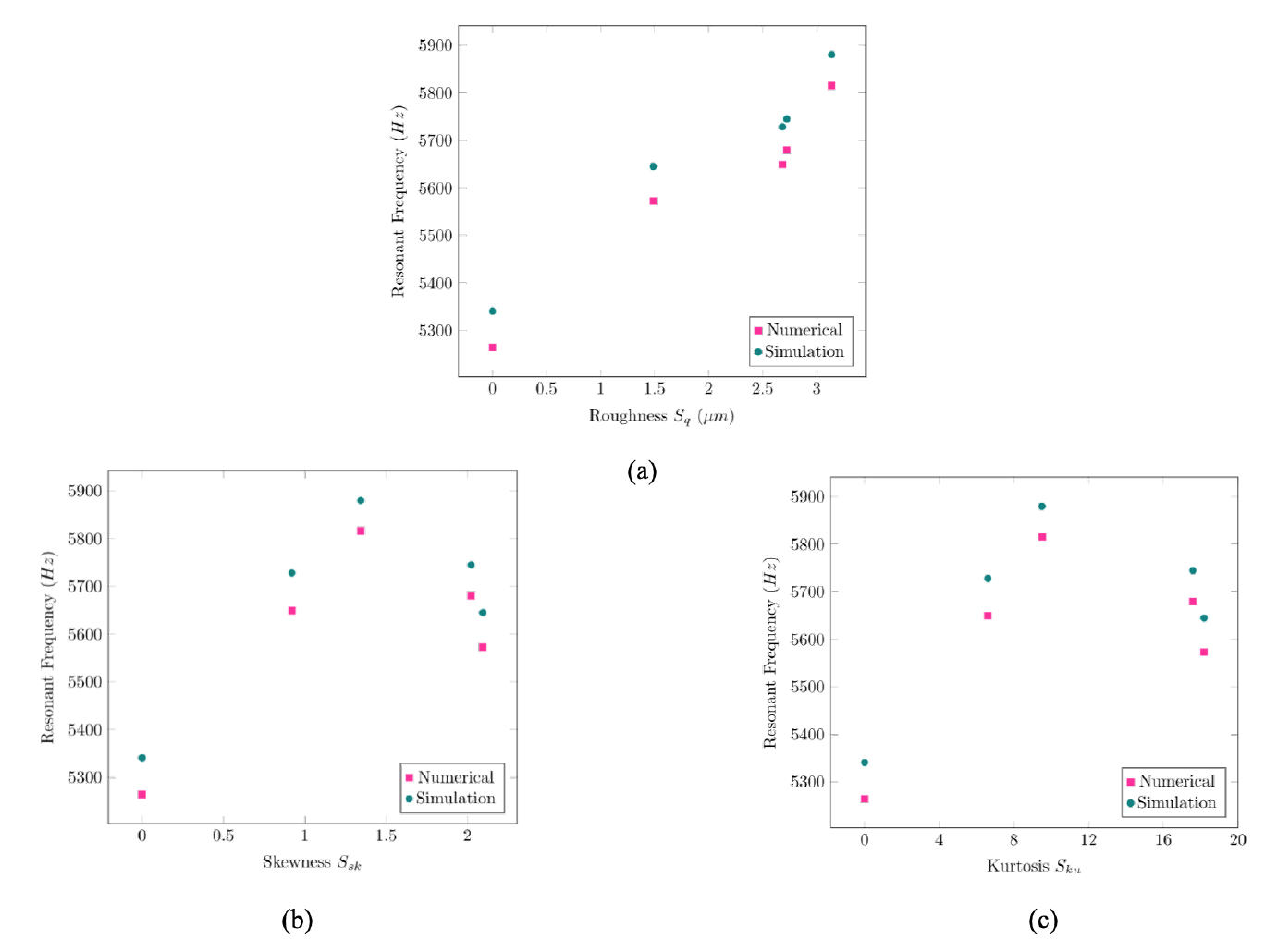
The four samples that were selected is plotted in figure 15. The first cantilever was set to have no roughness and is the ideal sample. The other four cantilevers were incorporated with roughness by having each sample roughness used in Table 3 to be on top of the 100 μm height of each beam, bounded inside T1. This was done to ensure each of the four cantilevers will have the same geometric (length, width and height) and material properties. In this way, the change of roughness can be evaluated fairly.
The computed frequency shows an increasing relationship with increasing roughness values indicating that if surface roughness is increased, the farther the beam frequency is from its designed resonant frequency. The relationship between the two computational methods showed a good agreement having around 1% error due to the following: mesh payloads, discretization of the geometry that represents its solution field, relative error in the computed eigenvalues, and limitation on algorithm's memory use in finding the solution to an eigenvalue problem during eigenfrequency study.
7. Conclusions
In this paper, surface roughness effects due to silicon DRIE on a cantilever beam energy harvester is studied using numerical and FEM modeling. Surface roughness was measured, characterized, and analyzed using a high-resolution 3D laser microscope. A depth etches of 550 μm results in a surface roughness of 1-4.7 μm at thickness of 100 μm. This roughness was incorporated in a 3D model cantilever beam and resonant frequency and output power were obtained using finite element method. It was found that roughness parameter ranging from 1.488-3.138 μm can significantly shift the resonant frequency by 5.53% to 9.48% or 308.31 Hz to 551.21 Hz of the device but does not have significant effect on the output power. Thus, the shift in resonant frequency must be considered in designing the fabrication process of energy harvesters so as to minimize the effects of surface roughness on the resonant frequency shift of the cantilever beams.
8. Acknowledgement
This research is funded by the Vibrational Energy Harvester for Resilient Sensor Nodes (VERSe) project under the Philippines’ Commission on Higher Education (CHED) – Philippine California Institutes (PCARI) program. The authors would like to acknowledge the contributions of the process engineers from the Marvell Nanofabrication Laboratory at the University of California-Berkeley.
References
[1] Hanqing Li Xiao Tan Tiantong Xu, Zhi Tao and Haiwang Li. Effects of deep reactive ion etching parameters on etching rate and surface morphology in extremely deep silicon etch process with high aspect ratio. Advances in Mechanical Engineering, 9(12):1–19, 06 2017.W.-K. Chen, Linear Networks and Systems (Book style) . Belmont, CA: Wadsworth, 1993, pp. 123–135. View Article
[2] Gong, Yuxuan and Xu, Jian and Buchanan, Relva, 2018, January, “Surface roughness: A review of its measurement at micro-/nano-scale”, volume 3, Physical Sciences Reviews, 10.1515/psr-2017-0057. View Article
[3] A.K. Pandey and R. Pratap. Coupled nonlinear effects of surface roughness on squeeze film damping in MEMS structures. Micromechanical. Microengineering, 14:14301437, 2004. View Article
[4] D. Mondal, R. Mukherjee, C. R. Chaudhuri. Comsol based multiphysics analysis of surface roughness effects on capacitance in RF MEMS varactors. Proceedings of the COMSOL Conference 2010 India, 2010.
[5] Wang, X., Kang, M., Fu, X., Li, C. Predictive modeling of surface roughness in lenses precision turning using regression and support vector machines. Int J. Adv Manuf Technol 87, 1273–1281 (2016). View Article
[6] Knud Lasse Lueth. State of the IOT 2018: Number of IOT devices now at market accelerating. IoT Analytics Research, 08 2018.
[7] A.G. Nejad and J.Y. Hasani. Effects of contact roughness and trapped free space on characteristics of rf-mems capacitive shunt switches. In 2015 IEEE International Conference on Electron Devices and Solid-State Circuits (EDSSC), pages 721-725, June 2015. View Article
[8] Raman A. Alam M.A. Palit, S. Implications of rough dielectric surfaces on charging-adjusted actuation of RF MEMS. IEEE Electron Device Letter,35, No. 9, 2014. View Article
[9] Dasgupta A. Nair D. Gopalakrishnan, S. Study of the effect of surface rough-ness on the performance of rf mems capacitive switches through 3d geometric modeling. Journal of the Electron Devices Society, 2016. View Article
[10] Huang, Xinlong & Zhenhui, Shen & Yang, Shuanqiang. (2018). Effect of Fabrication Parameters and Material Features on Surface Roughness of FDM Build Parts. 10.2991/jimec-18.2018.21. View Article
[11] H. Liu, J. W. McBride, and M. Z. M. Yusop. Surface characterization of an au/cnt composite for a MEMS switching application. pages 751–754, August 2016. View Article
[12] Manzano, J. M., De Leon, M. T., Magdaleno V. Jr., Rosales, M., Numerical Modeling of Surface Roughness Effects on the Natural Frequency of a Silicon Cantilever. EHST, No. 109, DOI: 10.11159/ehst20.109, November 2020 View Article
[13] D. Hochmann, E. Limoge, E. Bechhoefer, and D. Cihlar. Surface roughness and vibration study of an accelerometer mount used in a helicopter health usage and management system. 6:6–6, March 2002.
[14] E.S. Gadelmawla, M. Koura, T.M.A. Maksoud, H. Soliman, Roughness parameters. Journal of Materials Processing Technology, 123:133–145, 2002. View Article
[15] T. Schmidt M. Sun, H. and Boning D. Characterization and modeling of wafer and die level uniformity in deep reactive ion etching (drie). Mat. Res. Soc. Symp. Proc., 782, 2004. View Article
[16] Jurgensen C. W. Gottscho, R. and D. J. Vitkavage. Microscopic uniformity in plasma etching. Journal of Vacuum Science and Technology B: Microelectronics and Nanometer Structures Processing, 1992. View Article
[17] H.V. Jansen, M.J. Boer, S Unnikrishnan, M Louwerse, and M. Elwenspoek. Microscopic uniformity in plasma etching. Black silicon method X: A review on high speed and selective plasma etching of silicon with profile control: An in-depth comparison between Bosch and cryostat DRIE processes as a roadmap to next generation equipment, 19:033001, 02 2009. View Article
[18] J. Borneman, A. Kildishev, K. Chen, and V. Drachev. Fe modeling of surfaces with realistic 3d roughness: Roughness effects in optics of plasmonic nanoantennas. Proceedings of the COMSOL Conference 2009 Boston.